


MOSFETs, or Metal-Oxide-Semiconductor Field-Effect Transistors, are essential components in power electronics, used in everything from switches and amplifiers to energy converters.
Mosfet Structure:

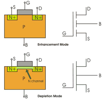
It is a four-terminal device with Source (S), Drain (D), Gate (G), and body (B) terminals. The body (B) is frequently connected to the source terminal, reducing the terminals to three. It works by varying the width of a channel along which charge carriers flow (electrons or holes).
The charge carriers enter the channel at the source and exit via the drain. The width of the channel is controlled by the voltage on an electrode called Gate which is located between the source and the drain. It is insulated from the channel near an extremely thin layer of metal oxide.
Different Types of MOSFET
MOSFET works in two modes
1. Depletion Mode: The transistor requires the Gate-Source voltage (VGS) to switch the device “OFF”. The depletion-mode MOSFET is equivalent to a “Normally Closed” switch.
2. Enhancement Mode: The transistor requires a Gate-Source voltage(VGS) to switch the device “ON”. The enhancement mode MOSFET is equivalent to a “Normally Open” switch.
Now with respect to the working principle, MOSFET is classified as follows:
P-Channel Depletion MOSFET
P-Channel Enhancement MOSFET
N-Channel Depletion MOSFET
N-Channel Enhancement MOSFET
P-Channel MOSFET

The drain and source are heavily doped p+ region and the substrate is in n-type. The current flows due to the flow of positively charged holes, and that’s why known as p-channel MOSFET.
When we apply negative gate voltage, the electrons present beneath the oxide layer experience repulsive force and are pushed downward into the substrate, the depletion region is populated by the bound positive charges which are associated with the donor atoms.
The negative gate voltage also attracts holes from the P+ source and drain region into the channel region.
N-Channel MOSFET
The drain and source are heavily doped N+ region and the substrate is p-type. The current flows due to the flow of negatively charged electrons and that’s why known as n-channel MOSFET.
When we apply the positive gate voltage, the holes present beneath the oxide layer experience repulsive force, and the holes are pushed downwards into the bound negative charges which are associated with the acceptor atoms.
The positive gate voltage also attracts electrons from the N+ source and drain region into the channel thus an electron-rich channel is formed.
There are several types of power MOSFETs designed to meet various application needs:
N-channel Power MOSFETs: Used for higher efficiency in applications requiring high current handling and high switching speeds.
P-channel Power MOSFETs: Typically used where simplicity of drive circuitry is needed since they require a negative gate-source voltage.
Dual MOSFETs: These contain both N-channel and P-channel MOSFETs in a single package, useful for compact designs.
Rugged MOSFETs: Specially designed to handle very high voltages and currents, often with enhanced protection features like improved avalanche breakdown resistance.
The working principle of a MOSFET depends upon the MOS capacitor. The MOS capacitor is the main part of MOS-FET. The semiconductor surface at the below oxide layer is located between the source and drain terminals. It can be inverted from p-type to n-type by applying positive or negative gate voltages.
When we apply positive gate voltage, the holes present under the oxide layer experience a repulsive force, and holes are pushed downward with the substrate.
The depletion region is populated by the bound negative charges that are associated with the acceptor atoms. The electrons reach, and the channel is formed. The positive voltage also attracts electrons from the n+ source and drain regions into the channel.
Now, if a voltage is applied between the drain and source, the current flows freely between the source and drain and the gate voltage controls the electrons in the channel. If we apply negative voltage, a hole channel will be formed under the oxide layer.
Applications
Amplifiers
Regulation for DC Motors
Constructions of Chopper Amplifiers
Switching and Amplifying Signals
One of the Topdiode most common power MOSFETs is the IRF540. It is widely used because it offers a good balance between performance and cost, making it suitable for a variety of power applications including switching power supplies and motor drives.
one of the Topdiode most famous MOSFETs is the IRF520. It is known for its versatility and reliability in various applications, including DIY electronics and industrial applications. It is frequently used in educational and hobbyist projects due to its ease of use and robustness.
Now more and more customer use our products to replace Infineon, AOS, Texas, we have better prices and better delivery. Technology is no problem.
Here following is our Top 10 hot selling mosfets.
NO# P/N & Package Cross to
1 TAP2305 SOT-23 Vishay SI2305
2 BSS84 SOT23 On semi/Diodes BSS84
3 2N7002 SOT-23 On semi/TI NDS7002A
4 TAP2302B SOT-23 On semi FDN327N
5 TP40P04K TO-252 Infineon PD50P04P4-13
6 TP3400 SOT-23 On semi NVTR4503N
7 TP3401 SOT-23 AOS AO3401
8 TP2333 SOT-23 Vishay SI2333DDS
9 TP2301 SOT-23 NXP NX2301PVL
10 TP3404 SOT-23 Diodes DMN3150L-7
For more interested products, please email to Loie sales4@topdiode.com